Graphene-Silicon Chip Breakthrough Paves Way for Post-Moore's Law Electronics
By Advanced Electronics Desk | April 2, 2025
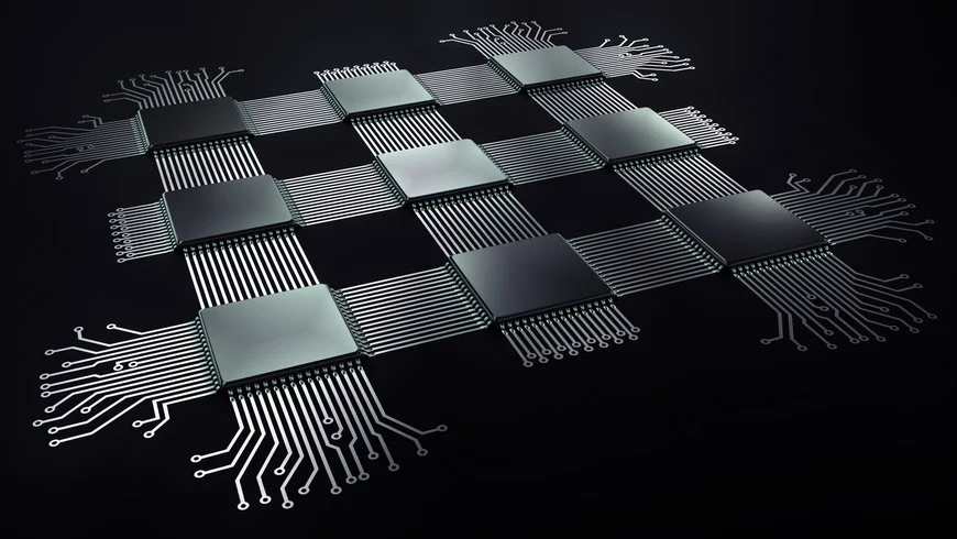
Researchers at the Massachusetts Institute of Technology (MIT) and the University of California, Berkeley have successfully integrated atomically-thin graphene with conventional silicon chip technology, creating a functional device that shows a tenfold improvement in certain key performance metrics. This hybrid approach, detailed in the journal Nature, is hailed as a critical step toward extending the life of Moore's Law and creating faster, more energy-efficient electronics.
Bridging Two Worlds: The 2D-3D Integration Challenge
For decades, the engine of the digital world has been the silicon transistor. As these transistors approach their physical limits, scientists have pinned hopes on two-dimensional materials like graphene—a single layer of carbon atoms renowned for its superb electrical conductivity and strength. However, a major hurdle has been integrating these fragile, nearly perfect 2D materials with the rough, three-dimensional landscape of a standard silicon chip without damaging their extraordinary properties.
The international team has now cracked this integration problem. They developed a novel, low-temperature fabrication process that allows them to "grow" high-quality graphene layers directly on top of pre-fabricated silicon components, creating a seamless connection. "Think of it like laying a perfect, ultra-thin sheet of diamond onto a complex LEGO structure without tearing it or creating gaps," explained Professor Alex Chen from MIT, a co-lead author of the study. "We've built a bridge between the future of materials and the manufacturing reality of today."
Demonstrated Performance and Immediate Applications
The prototype device, a specialized transistor called a heterojunction barristor, leverages graphene as an ultra-efficient tunable gate. This design allows for much faster switching speeds while operating at significantly lower voltages than pure silicon transistors. In tests, the hybrid chip component demonstrated electron mobility improvements of over an order of magnitude.
While not yet a replacement for the central processing unit (CPU), this technology has imminent, transformative applications. Its most significant initial impact is expected in the world of advanced sensors and high-frequency communications.
- 6G and Beyond: The technology could enable terahertz-frequency transceivers, essential for future ultra-high-speed wireless networks like 6G.
- Ultra-Sensitive Sensing: The graphene layer's sensitivity makes it ideal for next-generation environmental, biomedical, and imaging sensors capable of detecting single molecules.
- Lower Power Electronics: The efficiency gains directly translate to longer battery life for mobile and Internet of Things (IoT) devices.
A Pragmatic Path Forward for the Semiconductor Industry
This breakthrough is significant not just for its performance but for its practicality. The method is designed to be compatible with existing semiconductor fabrication plants (fabs) with minimal retooling. This offers a more feasible and cost-effective transition path compared to proposals requiring a complete overhaul of chip-making infrastructure.
"Industry doesn't need a revolution that throws out trillions of dollars of investment. It needs a smart evolution," said Dr. Sarah Miller from Berkeley. "Our work shows we can augment silicon, not just replace it, to get the performance boosts we desperately need for AI and data-centric computing."
The research consortium is now working with several major semiconductor foundries to scale up the process and test integration into more complex chip architectures. While full commercial deployment is likely several years away, this hybrid graphene-silicon platform marks a definitive turn from pure theoretical promise toward tangible technological reality.